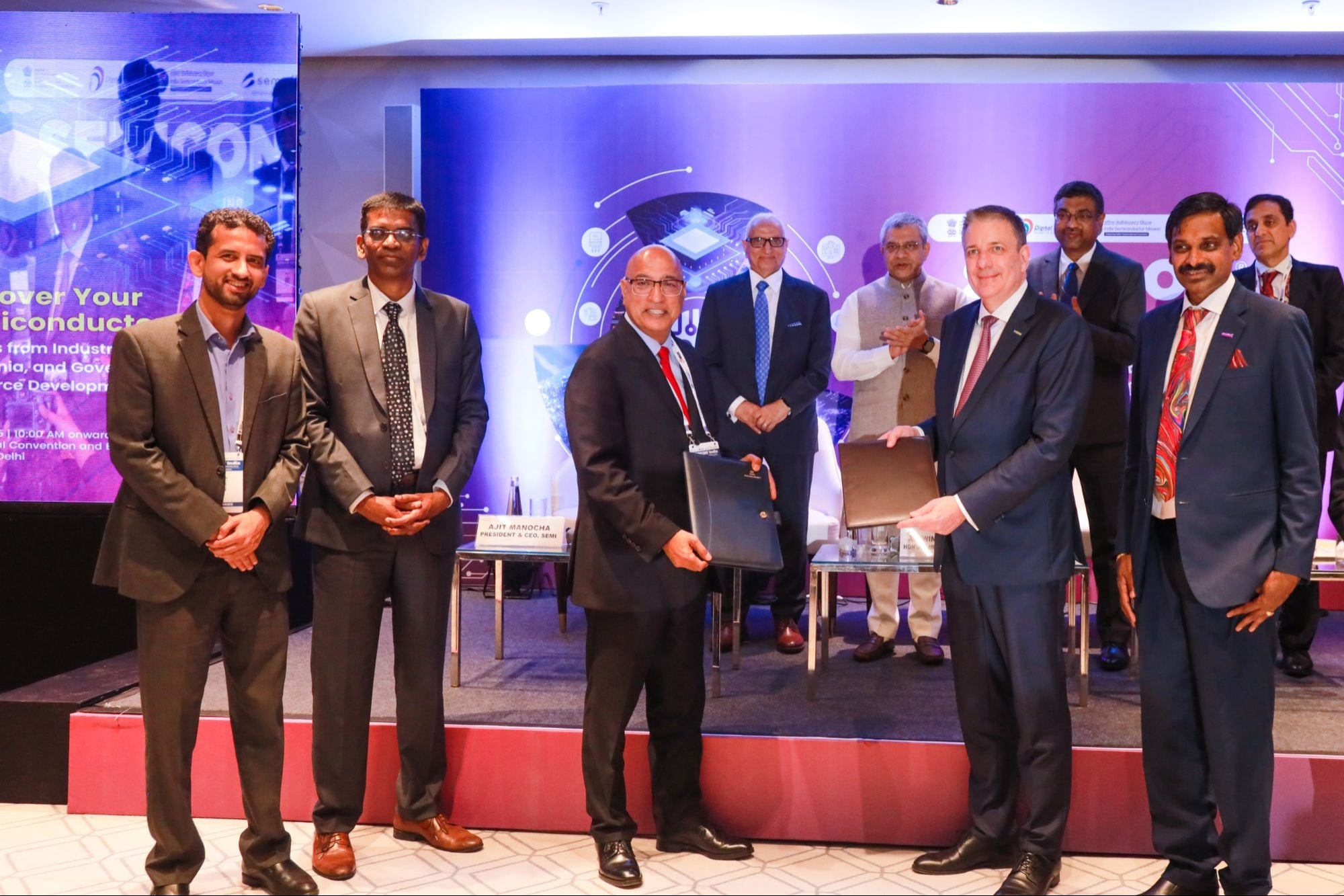
With Fab, OSAT & Design IP Ecosystem, Tata Electronics Strengthens Its Semiconductor Goals We will build a design IP ecosystem that empowers innovators across the country's semiconductor value chain from startups to established enterprises, says Dr Randhir Thakur, CEO & Managing Director, Tata Electronics
Opinions expressed by Entrepreneur contributors are their own.
You're reading Entrepreneur India, an international franchise of Entrepreneur Media.

With an eye on advancing the development of indigenous electronics & semiconductor solutions, and the design IP ecosystem, Tata Electronics and MeitY's Centre for Development of Advanced Computing (C-DAC) have signed an MoU. India accounts for around 20 per cent of the world's chip design engineers, placing it as a key player in the global semiconductor design ecosystem. Whether through PLI incentives or Design Linked Grants, India is offering end-to-end capabilities. The agreement marks a significant step forward for Tata Electronics and C-DAC in jointly building indigenous semiconductor design capabilities, thus strengthening the foundation for India's technological sovereignty.
Dr Randhir Thakur, CEO & Managing Director, Tata Electronics, said, "This partnership with C-DAC is an important step towards India's semiconductor self-sufficiency. By combining our advanced manufacturing capabilities with C-DAC's role as the nodal agency to strengthen India's domestic semiconductor chip design ecosystem, we will build a design IP ecosystem that empowers innovators across the country's semiconductor value chain, from startups to established enterprises. This aligns with our vision of building a trusted, end-to-end semiconductor value chain in India."
Tata Electronics is developing offerings across the entire semiconductor and electronics value chain, to serve global customers. The company is building India's first commercial Fab in Dholera, Gujarat, with a total investment of INR 91,000 crores (~US$11bn), and India's first indigenous Outsourced Semiconductor Assembly and Test (OSAT) facility in Jagiroad, Assam, with an investment of INR 27,000 crores (~US$3bn). Collectively, the plants will produce semiconductor solutions with applications across sectors, including automotive, mobile devices, artificial intelligence, defence, aerospace, and other key domains.
As the nodal agency implementing MeitY's Design Linked Incentive (DLI) Scheme and Chips to Startup (C2S) Programme, C-DAC has a mandate to nurture India's semiconductor design ecosystem. "Our partnership with Tata Electronics represents a crucial milestone in achieving this goal. Together, we will create a semiconductor design and IP ecosystem that provides domestic startups and academia with end-to-end support from silicon-proven IP portfolios to cutting-edge manufacturing capabilities. This collaboration will accelerate indigenous IP creation while positioning India as a leading global semiconductor design and manufacturing hub," said E. Magesh, Director General, C-DAC.
This development comes at a time when the Centre has finalised 25 priority semiconductor products that will be supported under the India Semiconductor Mission (ISM) to accelerate the creation of indigenous intellectual property (IP). Domestic IPs will help India transition from a manufacturing hub to an innovation partner in the global supply chain.
In May 2025, the Union Minister for Electronics & IT, Railways, and Information & Broadcasting, Ashwini Vaishnaw, inaugurated two state-of-the-art semiconductor design facilities in Noida and Bengaluru. These centres are India's first to focus on advanced 3-nanometer chip design, marking a significant milestone in the nation's semiconductor innovation journey. The DLI scheme, with a total outlay of INR 1000 crore promotes semiconductor design startups and MSMEs by offering financial support across product development stages. The scheme includes reimbursement of R&D costs, access to state-of-the-art design tools and incentives up to INR 15 crore per company to encourage innovation in chip design.


